










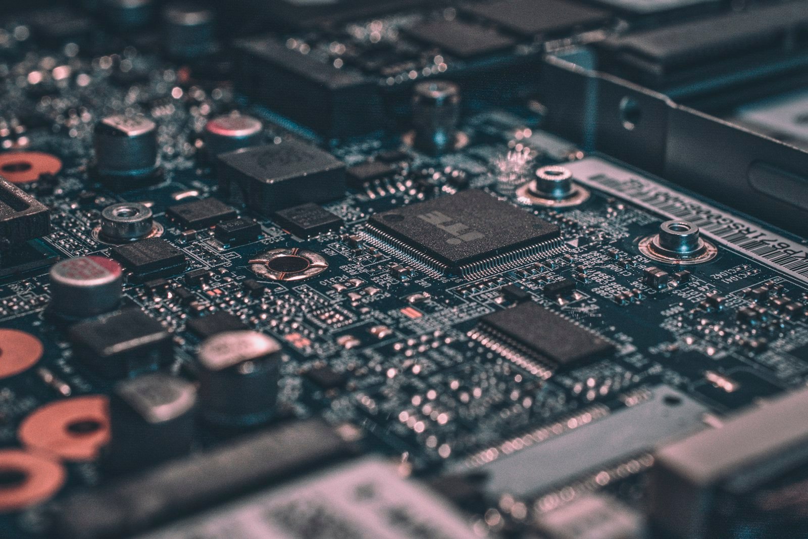
Semicon Mission 2.0 is the core development covered in this report. Below is a sourced breakdown of what is confirmed, what remains uncertain, and why it matters.
Why Semicon Mission 2.0 matters now
This section focuses on the practical implications of Semicon Mission 2.0 for readers following the story — what changed, what is confirmed, and what remains open.
India’s Union Cabinet on July 15, 2026, approved India Semiconductor Mission 2.0 with an outlay of Rs 1.27 lakh crore (Rs 1,27,500 crore), expanding the country’s chip strategy beyond fab incentives into design, materials, equipment, packaging, research and talent. Electronics and Information Technology Minister Ashwini Vaishnaw presented the package among a set of Cabinet and CCEA decisions that also included a Rs 62,500 crore Mobile Phone Manufacturing Scheme.
The government says Semicon Mission 2.0 is designed to attract around Rs 4 lakh crore of investment and support semiconductor and electronics production worth about Rs 2 lakh crore over the scheme period, with export upside near Rs 1 lakh crore in official briefings carried by The New Indian Express and The Hindu. The scheme duration is six years, according to The Indian Express.
What changes from Semicon 1.0
The first India Semiconductor Mission, launched in December 2021, carried a Rs 76,000 crore envelope. Under that phase, the government approved 12 projects with cumulative investments of around Rs 1.64 lakh crore across Gujarat, Assam, Andhra Pradesh, Uttar Pradesh and Odisha. Facilities linked to Tata Electronics, Micron, Kaynes Semicon and CG Semi are among those cited in July 2026 coverage; several packaging units in Sanand, Gujarat, had begun commercial production earlier in 2026.
ISM 2.0 recalibrates capital subsidies rather than simply copying the first scheme’s uniform 50% capex support. Reporting from The Indian Express and New Indian Express describes silicon fabs at 40% support; display and compound semiconductor fabs at 35%; advanced packaging at 35%; and conventional ATMP/OSAT at 25%. A 30% incentive is earmarked for manufacturing semiconductor equipment, chemicals, gases and materials, an explicit supply-chain expansion.
Design support can take the form of grants, equity co-investment or royalty-based funding. Research and talent pillars can receive up to 75% assistance with Centre and state participation, according to Vaishnaw’s briefing as reported by New Indian Express. Incentives are to be released on a pari-passu basis, matching private investment rather than front-loading cash.
The six pillars, in plain terms
- Chip design for strategic and commercial applications.
- Incentives for equipment, chemicals, gases and materials producers.
- Silicon fab support at the recalibrated 40% rate.
- Display and compound semiconductor fab support at 35%.
- Advanced and conventional packaging incentives at 35% and 25%.
- Heavy co-funding for R&D and workforce development, up to 75%.
Vaishnaw has said design is the first pillar and that India aims to be self-reliant in indigenous chip production by the end of the programme. That ambition sits against a global backdrop of memory tightness and AI-related demand for specialized silicon, conditions The Hindu noted when explaining why materials and gases suppliers are being courted now.
Why the Cabinet moved now
Policy makers have framed Semicon 2.0 as both industrial strategy and supply-chain insurance. The July Cabinet package arrived while West Asian conflict risks were disrupting energy and logistics assumptions for manufacturers. Localising electronics value chains (chips, phones, and critical materials) reduces exposure to shipping shocks and export-control swings.
India’s first-wave projects proved that large packaging and assembly commitments could be landed. The second wave tries to pull upstream: process chemicals, specialty gases, tools, and design IP that determine how much value stays onshore. Without that layer, India risks remaining an assembly destination rather than a full semiconductor ecosystem.
The parallel Mobile Phone Manufacturing Scheme underscores the demand-side logic. Handsets are a high-volume end market that can absorb domestic components if quality, cost and logistics align. Official notes summarized by The Hindu project large cumulative phone production over the scheme tenure and roughly 60,000 direct jobs from the mobile programme alone.
What companies and states should watch
Applicants will need bankable project plans that match the new incentive bands and the pari-passu disbursement model. States that already host ATMP/OSAT clusters, especially Gujarat’s Sanand corridor, may pursue materials and equipment parks next. Design-centric incentives could favor Bengaluru, Hyderabad and NCR talent pools if grant and equity windows are administered predictably.
Investors should separate headline outlay from cash timing. A Rs 1.27 lakh crore ceiling is not an overnight spend; it is a multi-year contingent liability against verified private capex. Execution risk remains high in fabs, where construction, utility reliability, water, and ultra-pure chemical supply decide yields as much as subsidy math.
Global peers are also racing for packaging and mature-node capacity. India’s pitch is policy continuity plus a larger domestic electronics market. Credibility will depend on transparent selection rounds, faster clearances, and evidence that first-wave plants ramp yields after commercial start.
Memory-market tightness cited in July briefings also strengthens the case for diversified capacity outside traditional East Asian hubs. If AI accelerators and consumer electronics continue to compete for packaging and substrate capacity, India’s ATMP base can capture overflow work even before leading-edge logic fabs mature. That sequencing (package and test first, deeper process capability later) matches what Semicon 1.0 already started and what 2.0 tries to complete with materials and design support.
Critics will ask whether lower percentage subsidies still compete with offers elsewhere in Asia and the United States. Supporters answer that India is pairing fiscal support with a huge domestic end market and with mobile-manufacturing incentives that can absorb locally finished chips. The next 12-18 months of approved project announcements will show which argument wins.
For context, the Cabinet’s July 15 decisions were not limited to chips. The same briefing cycle cleared the mobile scheme and other infrastructure items, signaling a broader localisation push while energy and logistics risk remained elevated because of West Asian conflict. Semicon 2.0 should therefore be read as one pillar of industrial policy rather than a standalone subsidy programme.
Multinationals weighing India against other destinations will parse three practical details: the six-year clock, the pari-passu cash schedule, and whether states add land, power and water packages that make the central rates competitive. Domestic conglomerates already active in Sanand and Dholera have first-mover operating experience; new entrants in chemicals and tools may be the true measure of whether the supply-chain pillar works.
FAQ
How large is Semicon Mission 2.0?
The Cabinet approved about Rs 1.27 lakh crore (Rs 1,27,500 crore) for a six-year programme, per July 15-16, 2026, coverage by major Indian dailies.
Are fab subsidies higher than before?
No. Coverage of ISM 2.0 describes lower percentage subsidies than the first scheme’s uniform 50% capex support, with silicon fabs at 40% and several other categories at 35% or 25%.
What results did Semicon 1.0 deliver?
Twelve projects were approved with roughly Rs 1.64 lakh crore of committed investment, and multiple packaging facilities had begun commercial production by early-mid 2026.
Primary sources
Related coverage on Topic Express
- India GDP Q2 Growth Data Highlights: 8.2%
- South Korea Stocks Plunge on AI Jitters
- FCC Bans New Foreign-Made Humanoid Robot Imports
- Business & Finance
Semicon Mission 2.0 is India’s attempt to convert early packaging wins into a fuller chip ecosystem covering design, materials, fabs and skills, backed by a larger fiscal envelope but tighter, more differentiated incentive rates. The Cabinet number is clear; the test will be how quickly bankable projects move from press note to production wafer.
Image: Photo via Unsplash (Unsplash License)
Related Topic Express coverage
- India GDP Q2 FY26: Why Real Growth Hit 8.2%
- Mobile Phone Manufacturing Scheme: India’s New ₹62,500 Cr Push